
 KAPSA Semicon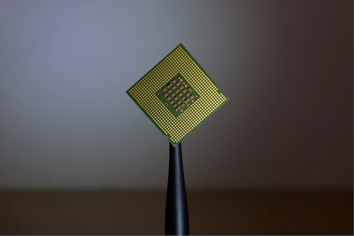
Overview
Whether you are validating first silicon, characterising a new product or screening production lots, reliable test data is the foundation of every decision. KAPSA Semicon provides semiconductor testing at wafer and package level for integrated circuits, discrete devices, power semiconductors and sensors.
We work from your datasheet, test specification or application requirements to build a test program that measures what matters — and flags marginal devices before they become field failures.
Capabilities
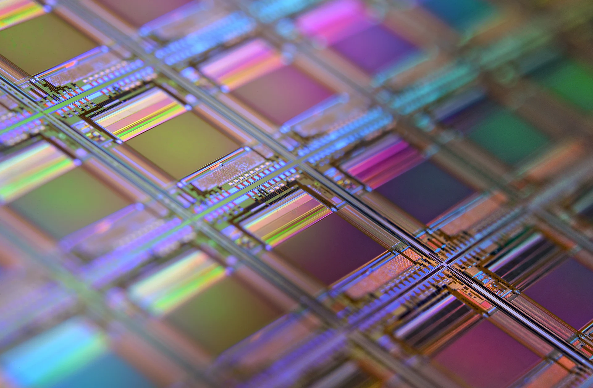
Wafer testing
Wafer-level electrical test and probing to identify good die and characterise process variation before assembly.
Package testing
Final electrical and functional test of packaged devices against datasheet limits.
Electrical testing
DC, AC and functional verification across voltage and temperature corners.
Parametric testing
Precise measurement of leakage, thresholds, on-resistance, timing and other key parameters.
Burn-in testing
Static and dynamic burn-in under elevated temperature and bias to screen out early-life (infant mortality) failures.
Production testing
Repeatable, high-throughput test flows for lot screening and outgoing quality assurance.
What you receive
- A documented test plan covering conditions, limits and sample sizes
- Test data with statistical summaries, distributions and pass/fail results
- Engineering commentary on outliers and marginal parameters
- Fast escalation to failure analysis when a device fails
Relevant standards
- JESD22-A108 (HTOL / burn-in)
- MIL-STD-883
- JESD47
- Customer datasheet & test specifications
Who it's for
Fabless design companies validating new silicon, IDMs and OSATs that need extra test capacity, and OEMs who want independent verification of incoming components. Testing often leads directly into reliability qualification.