
 KAPSA Semicon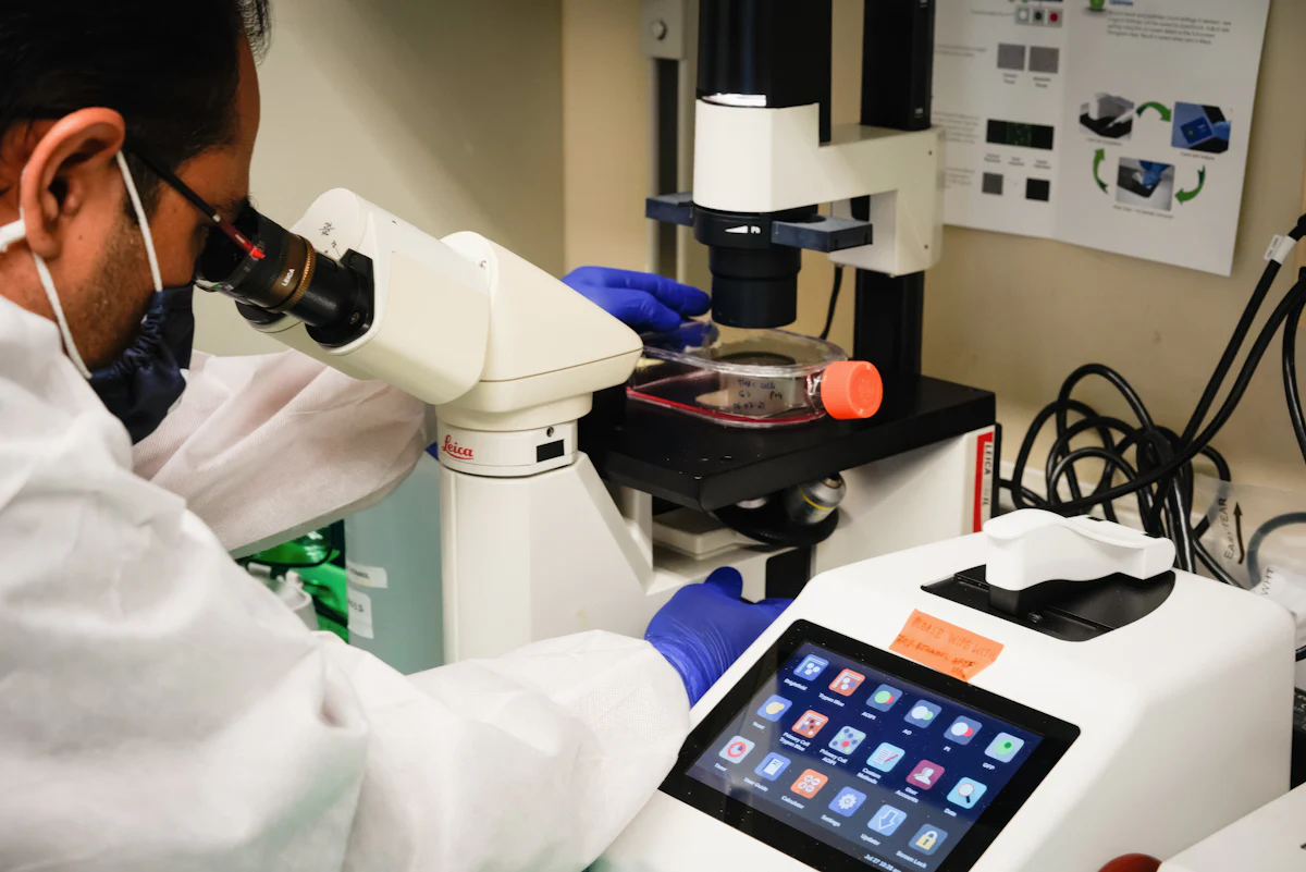
Overview
Many device failures and yield problems trace back to materials: contamination, incorrect plating, intermetallic growth or a compound that degrades under heat. Materials characterization gives you the elemental, structural and chemical evidence needed to act.
Our analyses support failure analysis, incoming material verification, supplier qualification and process development.
Capabilities
SEM-EDS
Scanning electron microscopy with energy-dispersive X-ray spectroscopy for high-resolution imaging and elemental mapping.
XRD
X-ray diffraction to identify crystalline phases, structure and residual stress.
XRF
X-ray fluorescence for non-destructive elemental composition and plating-thickness measurement.
FTIR
Fourier-transform infrared spectroscopy to identify organic materials, residues and polymers.
Optical microscopy
Bright-field, dark-field and polarised-light inspection for surface and cross-section analysis.
Contamination analysis
Combining techniques to identify foreign material, residues and corrosion products.
Typical applications
- Bond-pad and lead-frame contamination
- Plating composition and thickness
- Solder alloy and intermetallic analysis
- Mould compound and underfill identification
- RoHS screening of restricted elements
- Corrosion product identification
Who it's for
Process, quality and failure-analysis engineers, materials suppliers, and electronics manufacturers verifying incoming materials or investigating defects.