 KAPSA Semicon
Semiconductor Testing Lab
Electrical, parametric and functional testing at wafer and package level.
- Wafer & package test
- Parametric characterisation
- Production test

Laboratories
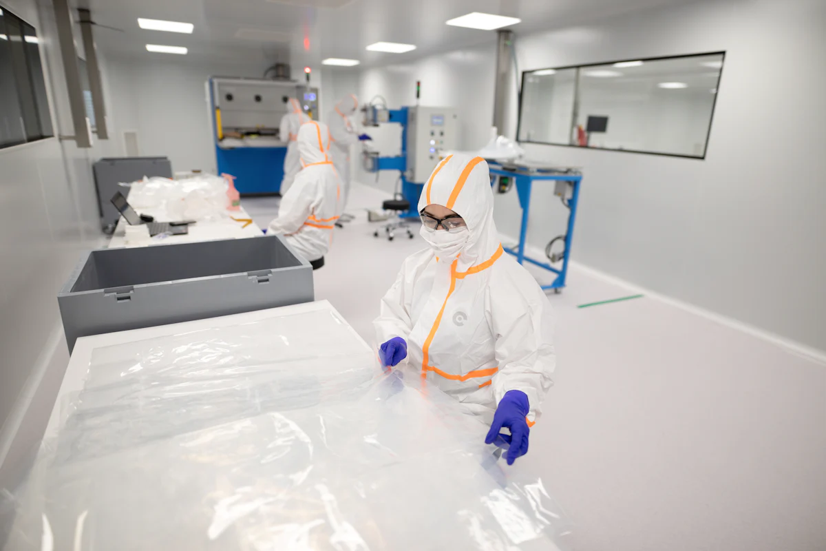
Our laboratories are organised so a device can move seamlessly from electrical test to stress testing to failure analysis — without leaving our hands or losing its history.
Our disciplines
Each laboratory discipline is run by specialists and operates under a common quality management system designed around ISO/IEC 17025.
Electrical, parametric and functional testing at wafer and package level.
Accelerated life and stress testing for qualification programmes.
Non-destructive and destructive analysis to identify root cause.
Climatic and mechanical stress to simulate real-world conditions.
Elevated temperature and bias screening to remove early-life failures.
Electromagnetic emissions and immunity testing for electronic products.
Elemental, structural and chemical analysis of materials.
Precise dimensional and physical measurement.
Traceable calibration of instruments and test equipment.
Integrated workflow
Because our labs work as one, a device that fails a reliability test goes straight to failure analysis — with its full electrical and stress history attached.
Accreditation
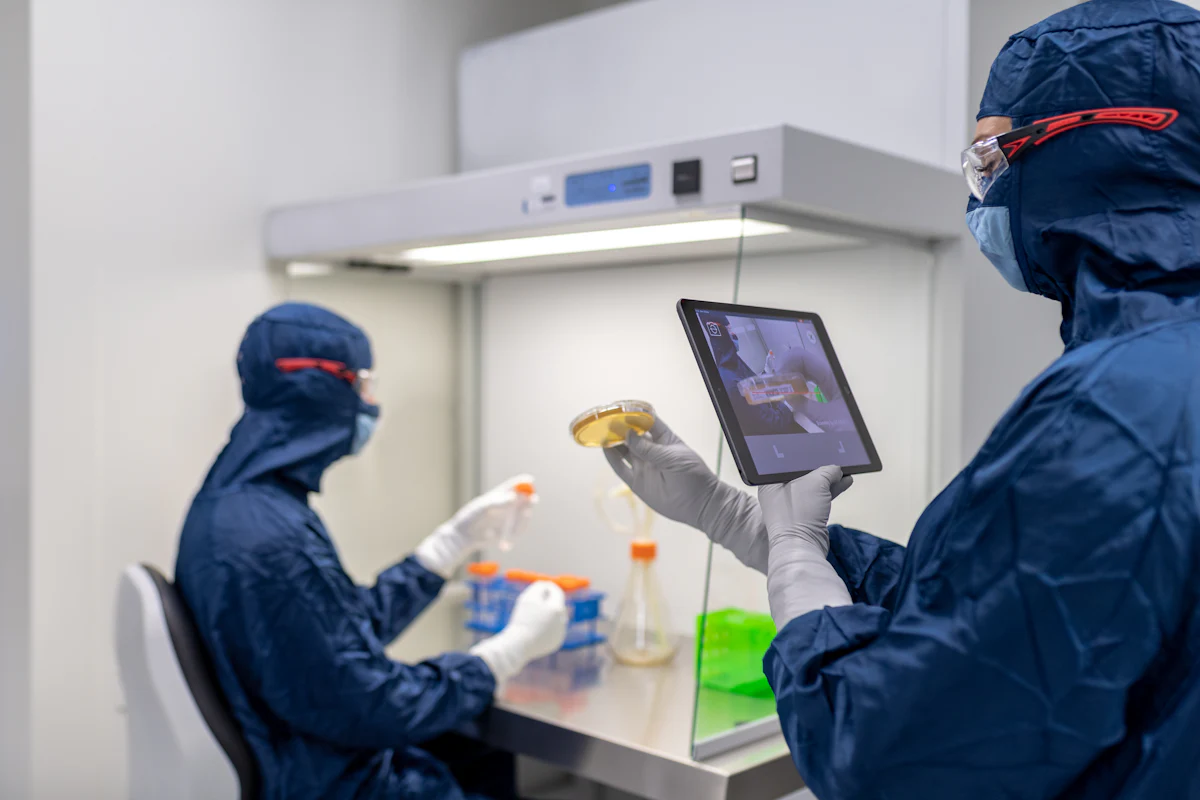
Our quality system is designed around ISO/IEC 17025, and we are pursuing NABL accreditation discipline by discipline — starting with reliability and failure analysis — to support recognition against frameworks such as JEDEC and AEC-Q100.
Share your requirement and our engineers will come back with a test plan, timeline and quotation — usually within one business day.